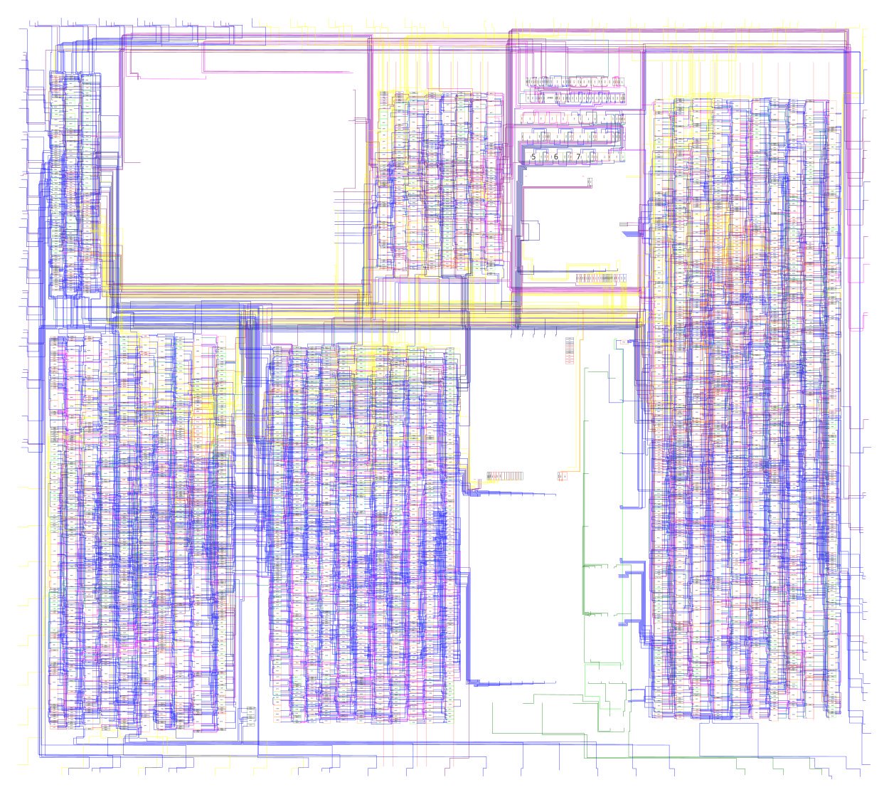
Furrtek, mostly known for his excellent work with Neo-Geo hardware and FPGA, just released a 36-page documentation depicting his process of reverse-engineering the original DMG-001.
In a 191-hour meticulous process, Furrtek was able to draw schematics for the following:
- All APU logic.
- All PPU logic.
- All I/O and timer logic.
- All DMA logic.
- All interrupt logic.
- Various stuff used for testing/debugging.
The main CPU though was left out of the equation at the moment due to it being “a standalone core which doesn’t use the standard cell topology” as explained by Furrtek.
All (important) DMG-CPU-B cells mapped and connected ! The final count is 3968. Hoping to get the schematics renderings shared in the next few hours, the editable files will come later. pic.twitter.com/JATexKcgui
— Furrtek (@furrtek) October 9, 2019
The schematics are up for grabs on Github, and will be converted to KiCad soon, hopefully, so anyone (with proper skills/knowledge) can edit the files.
Link for the GameBoy schematics: https://github.com/furrtek/DMG-CPU-Inside
